Thursday, December 31, 2009

First metallic nanoparticles resistant to extreme heat

Just as a gecko sheds its tail, metal-alloy particles endure 850 degrees Celsius by ditching weaker components, researchers report in Nature Materials

PITTSBURGH—A University of Pittsburgh team overcame a major hurdle plaguing the development of nanomaterials such as those that could lead to more efficient catalysts used to produce hydrogen and render car exhaust less toxic. The researchers reported Nov. 29 in Nature Materials the first demonstration of high-temperature stability in metallic nanoparticles, the vaunted next-generation materials hampered by a vulnerability to extreme heat.

Götz Veser, an associate professor and CNG Faculty Fellow of chemical and petroleum engineering in Pitt's Swanson School of Engineering, and Anmin Cao, the paper's lead author and a postdoctoral researcher in Veser's lab, created metal-alloy particles in the range of 4 nanometers that can withstand temperatures of more than 850 degrees Celsius, at least 250 degrees more than typical metallic nanoparticles.

Götz VeserForged from the catalytic metals platinum and rhodium, the highly reactive particles work by dumping their heat-susceptible components as temperatures rise, a quality Cao likened to a gecko shedding its tail in self-defense.

"The natural instability of particles at this scale is an obstacle for many applications, from sensors to fuel production,
" Veser said. "The amazing potential of nanoparticles to open up completely new fields and allow for dramatically more efficient processes has been shown in laboratory applications, but very little of it has translated to real life because of such issues as heat sensitivity. For us to reap the benefits of nanoparticles, they must withstand the harsh conditions of actual use."

Veser and Cao present an original approach to stabilizing metallic catalysts smaller than 5 nanometers. Materials within this size range boast a higher surface area and permit near-total particle utilization, allowing for more efficient reactions. But they also fuse together at around 600 degrees Celsius—lower than usual reaction temperatures for many catalytic processes—and become too large. Attempts to stabilize the metals have involved encasing them in heat-resistant nanostructures, but the most promising methods were only demonstrated in the 10- to 15-nanometer range, Cao wrote. Veser himself has designed oxide-based nanostructures that stabilized particles as small as 10 nanometers.

For the research in Nature Materials, he and Cao blended platinum and rhodium, which has a high melting point. They tested the alloy via a methane combustion reaction and found that the composite was not only a highly reactive catalyst, but that the particles maintained an average size of 4.3 nanometers, even during extended exposure to 850-degree heat. In fact, small amounts of 4-nanometer particles remained after the temperature topped 950 degrees Celsius, although the majority had ballooned to eight-times that size.

Veser and Cao were surprised to find that the alloy did not simply endure the heat. It instead sacrificed the low-tolerance platinum then reconstituted itself as a rhodium-rich catalyst to finish the reaction. At around 700 degrees Celsius, the platinum-rhodium alloy began to melt. The platinum "bled" from the particle and formed larger particles with other errant platinum, leaving the more durable alloyed particles to weather on. Veser and Cao predicted that this self-stabilization would occur for all metal catalysts alloyed with a second, more durable metal. ###

Veser and Cao conducted their work with support from the National Energy Technology Laboratory, the lead research and development office for the U.S. Department of Energy's (DOE) Office of Fossil Energy, as well as the DOE's Office of Basic Energy Sciences and the National Science Foundation.

Contact: Morgan Kelly mekelly@pitt.edu 412-624-4356 University of Pittsburgh

Wednesday, December 30, 2009

Scientists demonstrate multibeam, multi-functional lasers

Adaptable technology opens the door to a wide range of applications in chemical detection, climate monitoring and communications.

Cambridge, Mass – November 30, 2009 – An international team of applied scientists from Harvard, Hamamatsu Photonics, and ETH Zürich have demonstrated compact, multibeam, and multi-wavelength lasers emitting in the invisible part of the light spectrum (infrared). By contrast, typical lasers emit a single light beam of a well-defined wavelength. The innovative multibeam lasers have potential use in applications related to remote chemical sensing pollution monitoring, optical wireless, and interferometry.

Computer Render of a Multibeam, Multi-functional Laser

Caption: This is a computer rendering of one of the prototype multibeam, multi-functional lasers demonstrated by the team. The new laser emits several highly directional beams with the same wavelength near 8 microns, which requires two coherent beams: a probe beam and a reference beam. The probe beam interacts with a sample and recombines with the reference beam to reveal optical properties of the sample. A second type laser emits multiple small divergence beams with different wavelengths (9.3 and 10.5 microns) into different directions.

Credit: Federico Capasso and Nanfang Yu, Harvard School of Engineering and Applied Sciences. Usage Restrictions: None.
The research was led by postdoctoral researcher Nanfang Yu and Federico Capasso, Robert L. Wallace Professor of Applied Physics and Vinton Hayes Senior Research Fellow in Electrical Engineering, both at the Harvard School of Engineering and Applied Sciences (SEAS); Hirofumi Kan, General Manager of the Laser Group at Hamamatsu Photonics; and Jérôme Faist, Professor at ETH Zürich. The findings appeared online in the October 23 issue of Applied Physics Letters and will appear as a December 7 cover story.

"We have demonstrated devices that can create highly directional laser beams pointing in different directions either at the same or at different wavelengths," says Capasso. "This could have major implications for parallel high-throughput monitoring of multiple chemicals in the atmosphere or on the ground and be used, for example, for studying hazardous trace gases and aerosols, monitoring greenhouse gases, detecting chemical agents on the battlefield, and mapping biomass levels in forests."
The more versatile laser is a descendant of the quantum cascade laser (QCL), invented and first demonstrated by Capasso, Faist, and their collaborators at Bell Labs in 1994. Commercially available QCLs, made by stacking ultra-thin atomic layers of semiconductor materials on top of one another, can be custom designed to emit a well -defined infrared wavelength for a specific application or be made to emit simultaneously multiple wavelengths. To achieve multiple beams, the researchers patterned the laser facet with metallic structures that behave as highly directional antennas and then beam the light in different directions.

"Having multibeam and multi-wavelength options will provide unprecedented flexibility. The ability to emit multiple wavelengths is ideal for generating a quantitative map of the concentration of multiple chemicals in the atmosphere," explains Kan. "Profiles of these atmospheric components—as a function of altitude or location—are critically important for environmental monitoring, weather forecasting, and climate modeling." ###

The team's co-authors included graduate students Mikhail A. Kats and Markus Geiser, research associates Christian Pflügl, all from SEAS, and Qi Jie Wang, now an assistant professor at Nanyang Technical University in Singapore; researchers Tadataka Edamura, Shinichi Furuta, and Masamichi Yamanishi, all from Hamamatsu Photonics; and researchers Milan Fischer, Andreas Wittmann, both from the Institute of Quantum Electronics, ETH Zürich.

The work was partially supported by Air Force Office of Scientific Research and Harvard's Center for Nanoscale Systems (CNS), a member of the National Nanotechnology Infrastructure Network.

Contact: Michael Patrick Rutter mrutter@seas.harvard.edu 617-496-3815 Harvard University

Tuesday, December 29, 2009

Nanowires key to future transistors, electronics

WEST LAFAYETTE, Ind. - A new generation of ultrasmall transistors and more powerful computer chips using tiny structures called semiconducting nanowires are closer to reality after a key discovery by researchers at IBM, Purdue University and the University of California at Los Angeles.

The researchers have learned how to create nanowires with layers of different materials that are sharply defined at the atomic level, which is a critical requirement for making efficient transistors out of the structures.

"Having sharply defined layers of materials enables you to improve and control the flow of electrons and to switch this flow on and off," said Eric Stach, an associate professor of materials engineering at Purdue.

Nanowire Formation

Caption: Researchers are closer to using tiny devices called semiconducting nanowires to create a new generation of ultrasmall transistors and more powerful computer chips. The researchers have grown the nanowires with sharply defined layers of silicon and germanium, offering better transistor performance. As depicted in this illustration, tiny particles of a gold-aluminum alloy were alternately heated and cooled inside a vacuum chamber, and then silicon and germanium gases were alternately introduced. As the gold-aluminum bead absorbed the gases, it became "supersaturated" with silicon and germanium, causing them to precipitate and form wires.

Credit: Purdue University, Birck Nanotechnology Center/Seyet LLC. Usage Restrictions: None.
Electronic devices are often made of "heterostructures," meaning they contain sharply defined layers of different semiconducting materials, such as silicon and germanium. Until now, however, researchers have been unable to produce nanowires with sharply defined silicon and germanium layers. Instead, this transition from one layer to the next has been too gradual for the devices to perform optimally as transistors.

The new findings point to a method for creating nanowire transistors.

The findings are detailed in a research paper appearing Friday (Nov. 27) in the journal Science. The paper was written by Purdue postdoctoral researcher Cheng-Yen Wen, Stach, IBM materials scientists Frances Ross, Jerry Tersoff and Mark Reuter at the Thomas J. Watson Research Center in Yorktown Heights, N.Y, and Suneel Kodambaka, an assistant professor at UCLA's Department of Materials Science and Engineering.

Whereas conventional transistors are made on flat, horizontal pieces of silicon, the silicon nanowires are "grown" vertically. Because of this vertical structure, they have a smaller footprint, which could make it possible to fit more transistors on an integrated circuit, or chip, Stach said.

"But first we need to learn how to manufacture nanowires to exacting standards before industry can start using them to produce transistors," he said.

Nanowires might enable engineers to solve a problem threatening to derail the electronics industry.
New technologies will be needed for industry to maintain Moore's law, an unofficial rule stating that the number of transistors on a computer chip doubles about every 18 months, resulting in rapid progress in computers and telecommunications. Doubling the number of devices that can fit on a computer chip translates into a similar increase in performance. However, it is becoming increasingly difficult to continue shrinking electronic devices made of conventional silicon-based semiconductors.

"In something like five to, at most, 10 years, silicon transistor dimensions will have been scaled to their limit," Stach said.

Transistors made of nanowires represent one potential way to continue the tradition of Moore's law.

The researchers used an instrument called a transmission electron microscope to observe the nanowire formation. Tiny particles of a gold-aluminum alloy were first heated and melted inside a vacuum chamber, and then silicon gas was introduced into the chamber. As the melted gold-aluminum bead absorbed the silicon, it became "supersaturated" with silicon, causing the silicon to precipitate and form wires. Each growing wire was topped with a liquid bead of gold-aluminum so that the structure resembled a mushroom.

Then, the researchers reduced the temperature inside the chamber enough to cause the gold-aluminum cap to solidify, allowing germanium to be deposited onto the silicon precisely and making it possible to create a heterostructure of silicon and germanium.

The cycle could be repeated, switching the gases from germanium to silicon as desired to make specific types of heterostructures, Stach said.

Having a heterostructure makes it possible to create a germanium "gate" in each transistor, which enables devices to switch on and off. ###

The work is based at IBM's Thomas J. Watson Research Center and Purdue's Birck Nanotechnology Center in the university's Discovery Park and is funded by the National Science Foundation through the NSF's Electronic and Photonic Materials Program in the Division of Materials Research.

Writer: Emil Venere, (765) 494-4709, venere@purdue.edu Source: Eric Stach, (765) 494-1466, eastach@purdue.edu

Related Web site: Eric Stach: engineering.purdue.edu/MSE/People/

Sunday, December 27, 2009

Polymer with honeycomb structure

Empa scientists synthesize graphene-like material

Graphene consists of a two-dimensional carbon layer in which the carbon atoms are arranged on a hexagonal lattice, resembling a honeycomb. Carbon nanotubes are rolled-up sheets of graphene, and thick piles of graphene sheets form graphite. Graphene boasts some very special characteristics – it is extremely tear-resistant, an excellent thermal conductor, and reconciles such conflicting qualities as brittleness and ductility. In addition, graphene is impermeable to gases, which makes it interesting for applications involving air-tight membranes. Because of its unusual electronic properties graphene is viewed as a possible substitute material for silicon in semiconductor technologies.

STM Image of 2-D Porous Polymer

Caption: This is a scanning tunneling microscope image of the 2-D porous polymer (left side of image) with a model of the material structure superposed (right side: blue-green -- carbon; white -- hydrogen; gray -- silver surface).

Credit: © Empa. Usage Restrictions: Image may only be used with appropriate caption and credit.
By inserting holes of a specific size and distribution into graphene sheets, it should be possible to impart the material particular electronic characteristics. For these reasons intensive research is being conducted worldwide into the synthesis and characterization of two-dimensional graphene-like polymers. Graphene and graphene-like polymers are currently hot research topics in materials science, with this year's Körber European Science Award being awarded to the Dutch physicist Andre Geim for his pioneering studies in the field of two-dimensional carbon crystals.

New manufacturing method: "bottom-up" synthesis on metal surfaces
Together with colleagues from the Max Planck Institute for Polymer Research in Mainz, scientists from Empa's "nanotech@surfaces" laboratory have for the first time succeeded in synthesizing a graphene-like polymer with well defined pores. To achieve this feat the researchers allowed chemical building blocks of functionalized phenyl rings to "grow" spontaneously into a two-dimensional structure on a silver substrate. This created a porous form of graphene with pore diameters of a single atom and pore-to-pore spacings of less than a nanometer.

Until now, porous graphene has been manufactured using lithographic processes during which the holes are subsequently etched into the layer of material. These holes are, however, much larger than just a few atoms in diameter. They are also not as near to each other and significantly less precisely shaped as with the "bottom-up" technique based on molecular self-assembly developed by the Empa and Max Planck group. In this process the molecular building blocks join together spontaneously at chemically defined linking points to form a regular, two-dimensional network. This allows graphene-like polymers to be synthesized with pores, which are finer than is possible by any other technique.

Empa Research Award for Matthias Treier

The Empa Research Award 2009 goes to Matthias Treier, one of the authors of the publication about the synthesis of a graphene-like polymer.

One of the main goals of nanoscale research is to gain the ability to easily and reproducibly create chemically tailored, ordered and highly regular nanoscale objects. Among such structures, organic nanostructures are of particular interest since they are set to play an important role in future electronic devices. In his PhD thesis Matthias Treier has investigated several new approaches towards the bottom-up fabrication of organic nanostructures on single crystal metal surfaces. His «research objects» were besides graphene and graphene-like polymers so-called metallofullerenes.

First presented in 2003, the Empa Research Award is awarded today for the seventh time on the occasion of the PhD Symposium. Empa's Research Committee has evaluated a number of Master's theses, doctoral dissertations and scientific publications before selecting the outstanding work of Matthias Treier. ###

Contact: Beatrice Huber redaktion@empa.ch 41-448-234-733 Swiss Federal Laboratories for Materials Testing and Research (EMPA

Friday, December 25, 2009

Straightening messy correlations with a quantum comb

Teasing out unwanted knots in quantum communication, while keeping the information intact.

Quantum computing promises ultra-fast communication, computation and more powerful ways to encrypt sensitive information. But trying to use quantum states as carriers of information is an extremely delicate business. Now two physicists have shown, mathematically, how to gently tease out unwanted knots in quantum communication, while keeping the information intact. Their work is reported in the current issue of Physical Review Letters and highlighted with a Viewpoint in Physics (physics.aps.org/).

quantum entanglements

Caption: Physicists have shown that complicated quantum entanglements can be transformed into an arrangement where the entanglement fans out neatly from the hub qubit to each of the other qubits.

Credit: Dong Yang and Jens Eisert. Usage Restrictions: None.
When two particles are entangled, they effectively act as a single entity, even though they might be on opposite ends of the galaxy. Physicists can code information into particles to make quantum bits, or qubits, then entangle the qubits in an orderly fashion to form an entangled bit, or ebit. Ebits can then be used to create incredibly tough codes or teleport information between two distant systems. But messy entanglements among particles make qubits more susceptible to losing their encoded information.
Now Dong Yang and Jens Eisert of the University of Potsdam have shown how to delicately comb out a snarl of entanglements among many qubits while keeping the information intact. They designate one qubit as a hub and then use a combination of two existing quantum protocols to transform the original cat's cradle into an arrangement where entanglement fans out neatly from the hub qubit to each of the other qubits. This looks like a primitive model for a quantum World Wide Web: individual users each form an ebit with a single quantum search engine, and send queries and receive results via quantum teleportation. ###

Also in Physics: Staying or going? Chirality decides! Edward McCann writes a Viewpoint on the strange behavior of electrons in graphene, a single layer of carbon atoms.

Contact: James Riordon riordon@aps.org 301-209-3238 American Physical Society

Wednesday, December 23, 2009

Water droplets direct self-assembly process in thin-film materials

CHAMPAIGN, Ill. — You can think of it as origami – very high-tech origami.

Researchers at the University of Illinois have developed a technique for fabricating three-dimensional, single-crystalline silicon structures from thin films by coupling photolithography and a self-folding process driven by capillary interactions.

The films, only a few microns thick, offer mechanical bendability that is not possible with thicker pieces of the same material.

"This is a completely different approach to making three-dimensional structures," said Ralph G. Nuzzo, the G. L. Clark Professor of Chemistry at Illinois. "We are opening a new window into what can be done in self-assembly processes."

Spherical solar cells self-assembled from flower shaped flat Si leaflets

Spherical solar cells self-assembled from flower shaped flat Si leaflets with
thicknesses of 2 μm: (A) Schematic illustration of steps for fabricating a spherical shaped Si solar cell; (B) Optical image of a complete device consisting of the folded spherical Si shell, inner glass bead, and printed silver electrodes; (C) Magnified view of the silver wire connected to the top contact of the spherical device; (D) Current density (J) - voltage (V) characteristics of a spherical solar cell under AM1.5 simulated sunlight irradiation, with and without a white diffuse reflector.

Photo courtesy Ralph Nuzzo
Nuzzo is corresponding author of a paper accepted for publication in the Proceedings of the National Academy of Sciences. The paper is to be posted on the journal's Early Edition Web site the week of November 23.

As a demonstration of the new capillary-driven, self-assembly process, Nuzzo and colleagues constructed spherical and cylindrical shaped silicon solar cells and evaluated their performance.

The researchers also developed a predictive model that takes into account the type of thin film to be used, the film's mechanical properties and the desired structural shape.

"The model identifies the critical conditions for self-folding of different geometric shapes," said mechanical science and engineering professor K. Jimmy Hsia. "Using the model, we can improve the folding process, select the best material to achieve certain goals, and predict how the structure will behave for a given material, thickness and shape."
To fabricate their free-standing solar cells, the researchers began by using photolithography to define the desired geometric shape on a thin film of single-crystalline silicon, which was mounted on a thicker, insulated silicon wafer. Next, they removed the exposed silicon with etchant, undercut the remaining silicon foil with acid, and released the foil from the wafer. Then they placed a tiny drop of water at the center of the foil pattern.

As the water evaporated, capillary forces pulled the edges of the foil together, causing the foil to wrap around the water droplet.

To retain the desired shape after the water had fully evaporated, the researchers placed a tiny piece of glass, coated with an adhesive, at the center of the foil pattern. The glass "froze" the three-dimensional structure in place, once it had reached the desired folded state.

"The resulting photovoltaic structures, not yet optimized for electrical performance, offer a promising approach for efficiently harvesting solar energy with thin films," said Jennifer A. Lewis, the Thurnauer Professor of Materials Science and Engineering and director of the university's Frederick Seitz Materials Research Laboratory.

Unlike conventional, flat solar cells, the curved, three-dimensional structures also serve as passive tracking optics by absorbing light from nearly all directions.

"We can look forward from this benchmark demonstration to photovoltaic structures made from thin films that behave as though they are optically dense, and much more efficient," Lewis said.
The new self-assembly process can be applied to a variety of thin-film materials, not just silicon, the researchers noted in their paper. ###

With Nuzzo, Hsia and Lewis, co-authors of the paper are graduate students Xiaoying Guo and Huan Li, and postdoctoral researchers Bok Yeop Ahn and Eric B. Douss.

Hsia is associate dean of the Graduate College and is affiliated with the university's Micro and Nanotechnology Laboratory.

Lewis is affiliated with the department of chemical and biomolecular engineering and the Micro and Nanotechnology Laboratory.

Nuzzo is affiliated with the Institute for Genomic Biology, the Micro and Nanotechnology Laboratory, the materials science and engineering department, and the Frederick Seitz Materials Research Laboratory.

The U.S. Defense Advanced Research Projects Agency, the Department of Energy and the National Science Foundation funded the work.

Contact: James E. Kloeppel kloeppel@illinois.edu 217-244-1073 University of Illinois at Urbana-Champaign

Tuesday, December 22, 2009

Nanotube defects equal better energy and storage systems

Most people would like to be able to charge their cell phones and other personal electronics quickly and not too often. A recent discovery made by UC San Diego engineers could lead to carbon nanotube-based supercapacitors that could do just this.

In recent research, published in Applied Physics Letters, Prabhakar Bandaru, a professor in the UCSD Department of Mechanical and Aerospace Engineering, along with graduate student Mark Hoefer, have found that artificially introduced defects in nanotubes can aid the development of supercapacitors.

"While batteries have large storage capacity, they take a long time to charge; while electrostatic capacitors can charge quickly but typically have limited capacity. However, supercapacitors/electrochemical capacitors incorporate the advantages of both," Bandaru said.

Mark Hoefer and Prab Bandaru, University of California - San Diego

Caption: Mark Hoefer (left), a UCSD materials science grad student, and mechanical engineering professor Prabhakar Bandaru have discovered that defects in carbon nanotubes could lead to supercapacitors that could possibly be used for portable electronic devices such as cell phones.

Credit: UC San Diego, Usage Restrictions: Credit UC San Diego.

Nanotube

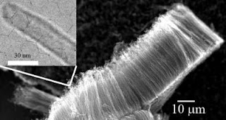
Caption: Carbon nanotubes could serve as supercapacitor electrodes with enhanced charge and energy storage capacity (inset: a magnified view of a single carbon nanotube).

Credit: UC San Diego. Usage Restrictions: Credit UC San Diego.
Carbon nanotubes (CNTs) have been generally hailed as one of the wonder materials of the 21st century and have been widely recognized as ushering in the nanotechnology revolution. They are cylindrical structures, with diameters of 1 to 100 nanometers, that have been suggested to have outstanding structural, chemical, and electrical, characteristics based on their atomically perfect structures with a large surface area-to-volume ratio. However, defects are inevitable in such a practical structure, an aspect that was first investigated by UCSD engineering graduate student Jeff Nichols and then substantially extended by Hoefer in Bandaru's lab.

"We first realized that defective CNTs could be used for energy storage when we were investigating their use as electrodes for chemical sensors," Hoefer said. "During our initial tests we noticed that we were able to create charged defects that could be used to increase CNT charge storage capabilities."

Specifically, defects on nanotubes create additional charge sites enhancing the stored charge. The researchers have also discovered methods which could increase or decrease the charge associated with the defects by bombarding the CNTs with argon or hydrogen.

"It is important to control this process carefully as too many defects can deteriorate the electrical conductivity, which is the reason for the use of CNTs in the first place. Good conductivity helps in efficient charge transport and increases the power density of these devices," Bandaru added.
"At the very outset, it is interesting that CNTs, which are nominally considered perfect, could be useful with so many incorporated defects," he added.

The researchers think that the energy density and power density obtained through their work could be practically higher than existing capacitor configurations which suffer from problems associated with poor reliability, cost, and poor electrical characteristics.

Bandaru and Hoefer hope that their research could have major implications in the area of energy storage, a pertinent topic of today. "We hope that our research will spark future interest in utilizing CNTs as electrodes in charge storage devices with greater energy and power densities," Hoefer said.

While more research still needs to be done to figure out potential applications from this discovery, the engineers suggest that this research could lead to wide variety of commercial applications, and hope that more scientists and engineers will be compelled to work in this area, Bandaru said.

Meanwhile, Hoefer said this type of research will help fuel his future engineering career.

"It is remarkable how current tools and devices are becoming increasing more efficient and yet smaller due to discoveries made at the nanoscale," he said. "My time spent investigating CNTs and their potential uses at the Jacobs School will prepare me for my career, since future research will continue the trend of miniaturization while increasing efficiency." ###

"Determination and enhancement of the capacitance contributions in carbon nanotube based electrode systems," Applied Physics Letters. M. Hoefer and P.R. Bandaru, Department of Mechanical and Aerospace Engineering, Materials Science Program, University of California, San Diego.

Contact: Andrea Siedsma asiedsma@soe.ucsd.edu 858-822-0899 University of California - San Diego

Monday, December 21, 2009

Small nanoparticles bring big improvement to medical imaging

If you're watching the complex processes in a living cell, it is easy to miss something important—especially if you are watching changes that take a long time to unfold and require high-spatial-resolution imaging. But new research* makes it possible to scrutinize activities that occur over hours or even days inside cells, potentially solving many of the mysteries associated with molecular-scale events occurring in these tiny living things.

A joint research team, working at the National Institute of Standards and Technology (NIST) and the National Institute of Allergy and Infectious Diseases (NIAID), has discovered a method of using nanoparticles to illuminate the cellular interior to reveal these slow processes.

Nanoparticles for Medical Imaging

Caption: Human red blood cells, in which membrane proteins are targeted and labeled with quantum dots, reveal the clustering behavior of the proteins. The number of purple features, which indicate the nuclei of malaria parasites, increases as malaria development progresses. The NIST logo at bottom was made by a photo lithography technique on a thin film of quantum dots, taking advantage of the property that clustered dots exhibit increased photoluminescence. (White bars: 1 micrometer; red: 10 micrometer.)

Credit: NIST. Usage Restrictions: None.
Nanoparticles, thousands of times smaller than a cell, have a variety of applications. One type of nanoparticle called a quantum dot glows when exposed to light. These semiconductor particles can be coated with organic materials, which are tailored to be attracted to specific proteins within the part of a cell a scientist wishes to examine.

"Quantum dots last longer than many organic dyes and fluorescent proteins that we previously used to illuminate the interiors of cells," says biophysicist Jeeseong Hwang, who led the team on the NIST side. "They also have the advantage of monitoring changes in cellular processes while most high-resolution techniques like electron microscopy only provide images of cellular processes frozen at one moment.
Using quantum dots, we can now elucidate cellular processes involving the dynamic motions of proteins."

For their recent study, the team focused primarily on characterizing quantum dot properties, contrasting them with other imaging techniques. In one example, they employed quantum dots designed to target a specific type of human red blood cell protein that forms part of a network structure in the cell's inner membrane. When these proteins cluster together in a healthy cell, the network provides mechanical flexibility to the cell so it can squeeze through narrow capillaries and other tight spaces. But when the cell gets infected with the malaria parasite, the structure of the network protein changes.

"Because the clustering mechanism is not well understood, we decided to examine it with the dots," says NIAID biophysist Fuyuki Tokumasu. "We thought if we could develop a technique to visualize the clustering, we could learn something about the progress of a malaria infection, which has several distinct developmental stages."

The team's efforts revealed that as the membrane proteins bunch up, the quantum dots attached to them are induced to cluster themselves and glow more brightly, permitting scientists to watch as the clustering of proteins progresses. More broadly, the team found that when quantum dots attach themselves to other nanomaterials, the dots' optical properties change in unique ways in each case. They also found evidence that quantum dot optical properties are altered as the nanoscale environment changes, offering greater possibility of using quantum dots to sense the local biochemical environment inside cells.

"Some concerns remain over toxicity and other properties," Hwang says, "but altogether, our findings indicate that quantum dots could be a valuable tool to investigate dynamic cellular processes." ###

* H. Kang, F. Tokumasu, M. Clarke, Z. Zhou, J. Tang, T. Nguyen and J. Hwang. Probing dynamic fluorescence properties of single and clustered quantum dots towards quantitative biomedical imaging of cells. WIREs Nanomedicine and Nanobiotechnology. Early view online at wires.wiley.com/WileyCDA/WiresIssue/.

Contact: Chad Boutin boutin@nist.gov 301-975-4261 National Institute of Standards and Technology (NIST)

Sunday, December 20, 2009

'No muss, no fuss' miniaturized analysis for complex samples developed

The goal of an integrated, miniaturized laboratory analysis system, also known as a "lab-on-a-chip," is simple: sample in, answer out. However, researchers wanting to use these microfluidic devices to analyze complex solutions containing particulates or other contaminating materials often find that the first part of the process isn't so easy. Effective sample preparation from these solutions can be laborious, expensive and time-consuming, involving complicated laboratory methods that must be performed by skilled technicians. This can significantly diminish the benefits associated with using miniaturized analytical techniques. Recent work at the National Institute of Standards and Technology (NIST) could help change that.

NIST researchers Elizabeth Strychalski and David Ross, in collaboration with Alyssa Henry of Applied Research Associates Inc. (Alexandria, Va.), have developed a novel and simple way to analyze samples that are complex mixtures, such as whole milk, blood serum and dirt in solution.

Schematic of NIST GEMBE Sample Analyzer

Caption: The NIST GEMBE microfluidic sample analysis system is shown schematically.

Credit: E. Strychalski and D. Ross, NIST, and A. Henry, ARA Inc. Usage Restrictions: Must be run with 2nd photo accompanying this story.

Complex Samples Analyzed by NIST GEMBE System

Caption: These photographs show three complex samples that can be successfully analyzed by the technique: (b) whole milk, (c) dirt and (d) coal fly ash.

Credit: E. Strychalski and D. Ross, NIST, and A. Henry, ARA Inc. Usage Restrictions: Must be run with 1st image accompanying this story.
In a paper published recently in Analytical Chemistry,* the team describes its latest enhancement to a NIST-developed separation technique called gradient elution moving boundary electrophoresis (GEMBE) (see "New Miniaturized Device for Lab-on-a-Chip Separations" in NIST Tech Beat, Jan. 19, 2007).

GEMBE relies on a combination of electrophoresis and variable pressure-driven flow through a microchannel. Electrophoresis uses electricity to push a mixture in solution through a channel, forcing the individual components to separate as they move at specific rates based on their individual properties, such as size and electrical charge. Complex samples can be difficult to separate cleanly because components in these samples (for example, the fat globules in milk or proteins in blood) can "foul" microfluidic channels in a way that prevents reliable detection of the desired sample components.

The new technique solves this problem by pumping a buffer solution under controlled pressure in the opposite direction. This opposing pressure flow acts as a "fluid gate" between the sample reservoir and the microchannel. Gradually reducing the pressure of the counterflow opens the "gate" a little bit at a time.
A specific sample component is detected when the pressure flow becomes weak enough—when the "gate" opens wide enough—that the component's electrophoretic motion pushes it against the pressure flow and into the channel for detection. In this way, different components enter the channel at different times based on their particular electrophoretic motion. Most importantly, the channel doesn't become fouled because the unwanted material in the sample is held out during the analysis by the pressure flow.

In their paper, the researchers validated their GEMBE analysis technique by testing it with solutions of whole milk, dirt, estuarine sediment, coal fly ash, pulverized leaves and blood serum. In all cases—and without the muss and fuss of pre-analysis sample preparation—the system was able to reproducibly separate and quantify specific components from the solutions, including potassium, calcium, sodium, magnesium, lithium and melamine.

"GEMBE is well-suited to the microfluidic analysis of 'real-world' samples," Strychalski says. "We have shown that the method can handle solutions containing particulates, proteins and other materials that would confound the majority of other microfluidic techniques."

Because of its ability to easily and rapidly characterize complex mixtures with minimal preparation, the researchers believe that GEMBE shows enormous promise for diverse applications, such as monitoring contaminants in food or water supplies, determining nutrient levels in soil, detecting biochemical warfare agents, and diagnosing medical conditions. The next steps, they say, are to miniaturize the desktop equipment now used in the system and integrate all of the parts to develop a true "lab-on-a-chip" field analyzer that can rival the effectiveness of a full-scale facility. ###

* E. Strychalski, A. Henry and D. Ross. Microfluidic analysis of complex samples with minimal sample preparation using Gradient Elution Moving Boundary Electrophoresis. Analytical Chemistry, Vol. 81, No. 24, Dec. 15, 2009; published online Nov. 10, 2009.

Contact: Michael E. Newman michael.newman@nist.gov 301-975-3025 National Institute of Standards and Technology (NIST)

Friday, December 18, 2009

Small optical force can budge nanoscale objects

ITHACA, N.Y. - With a bit of leverage, Cornell researchers have used a very tiny beam of light with as little as 1 milliwatt of power to move a silicon structure up to 12 nanometers. That's enough to completely switch the optical properties of the structure from opaque to transparent.

The technology could have applications in the design of micro-electromechanical systems (MEMS) – nanoscale devices with moving parts – and micro-optomechanical systems (MOMS) which combine moving parts with photonic circuits, said Michal Lipson, associate professor of electrical and computer engineering.

The research by postdoctoral researcher Gustavo Wiederhecker, Long Chen Ph.D. '09, Alexander Gondarenko, Ph.D. '10, and Lipson appears in the online edition of the journal Nature and will appear in a forthcoming print edition.

Scanning electron micrograph of two thin, flat rings of silicon nitride

Scanning electron micrograph of two thin, flat rings of silicon nitride, each 190 nanometers thick and mounted a millionth of a meter apart. Light is fed into the ring resonators from the straight waveguide at the right. Under the right conditions optical forces between the two rings are enough to bend the thin spokes and pull the rings toward one another, changing their resonances enough to act as an optical switch. Cornell Nanophotonics Group
Light can be thought of as a stream of particles that can exert a force on whatever they strike. The sun doesn't knock you off your feet because the force is very small, but at the nanoscale it can be significant. "The challenge is that large optical forces are required to change the geometry of photonic structures," Lipson explained.

But the researchers were able to reduce the force required by creating two ring resonators – circular waveguides whose circumference is matched to a multiple of the wavelength of the light used – and exploiting the coupling between beams of light traveling through the two rings.

A beam of light consists of oscillating electric and magnetic fields, and these fields can pull in nearby objects, a microscopic equivalent of the way static electricity on clothes attracts lint.
This phenomenon is exploited in "optical tweezers" used by physicists to trap tiny objects. The forces tend to pull anything at the edge of the beam to be pulled toward the center.

When light travels through a waveguide whose cross-section is smaller than its wavelength some of the light spills over, and with it the attractive force. So parallel waveguides close together, each carrying a light beam, are drawn even closer, rather like two streams of rainwater on a windowpane that touch and are pulled together by surface tension.

The researchers created a structure consisting of two thin, flat silicon nitride rings about 30 microns (millionths of a meter) in diameter mounted one above the other and connected to a pedestal by thin spokes. Think of two bicycle wheels on a vertical shaft, but each with only four thin, flexible spokes. The ring waveguides are three microns wide and 190 nanometers (nm – billionths of a meter) thick, and the rings are spaced 1 micron apart.

When light at a resonant frequency of the rings, in this case infrared light at 1533.5 nm, is fed into the rings, the force between the rings is enough to deform the rings by up to 12 nm, which the researchers showed was enough to change other resonances and switch other light beams traveling through the rings on and off.

When light in both rings is in phase – the peaks and valleys of the wave match – the two rings are pulled together. When it is out of phase they are repelled. The latter phenomenon might be useful in MEMS, where an ongoing problem is that silicon parts tend to stick together, Lipson said.

An application in photonic circuits might be to create a tunable filter to pass one particular optical wavelength, Wiederhecker suggested. ###

The work is supported by the National Science Foundation (NSF) and the Cornell Center for Nanocale Systems. Devices were fabricated at the Cornell NanoScale Science and Technology Facility, also supported by NSF.

Contact: Blaine Friedlander bpf2@cornell.edu 607-254-8093 Cornell University

Thursday, December 17, 2009

NJIT engineer discovers why particles disperse on liquids

Even if you are not a cook, you might have wondered why a pinch of flour (or any small particles) thrown into a bowl of water will disperse in a dramatic fashion, radiating outward as if it was exploding. Pushpendra Singh, PhD, a mechanical engineering professor at NJIT who has studied and written about the phenomenon, has not only thought about it, but can explain why.

He says that what's known as the "repulsive hydrodynamic force arising from the oscillation of particles" causes them to disperse. A particle trapped in a liquid surface vibrates up and down from its equilibrium position on the surface, or interface, where air meets water. When many particles do this simultaneously, an explosive dispersion occurs.

Pushpendra Singh, New Jersey Institute of Technology

Caption: NJIT's Pushpendra Singh (right) and his graduate student examine particles in a dish.

Credit: New Jersey Institute of Technology. Usage Restrictions: None.
"Spontaneous Dispersion of Particles on Liquid Surfaces," which appeared in the Nov. 11, 2009 early edition of the Proceedings of the National Academy of Sciences explains the theory. The National Science Foundation has supported this research.

Singh says that when small particles, such as flour or pollen, come in contact with a liquid surface, they immediately disperse and form a monolayer. The dispersion occurs so quickly that it appears explosive, especially on the surface of liquids like water.
This explosive dispersion is a consequence of the capillary force pulling particles towards their equilibrium positions in the interface. The capillary force causes the particles to accelerate very rapidly.

"If a particle barely touches the interface, it is pulled onto the surface," said Singh. "For example, if the contact angle for a spherical particle is 90 degrees, it floats in the state of equilibrium so that one-half of it is above the surface and the remaining half is below. If the particle, however, is not in this position, the capillary force will force it to be."

What's interesting is that the smaller the particles, the faster they move. For nanometer-sized particles like viruses and proteins, the velocity or speed on an air-water interface can be as high as 167 kilometers (about 100 miles) per hour.

Singh says the motion of the particles is dominated by inertia because the viscous damping—which is like friction—is too small. He compares the situation to a moving pendulum. "The pendulum will oscillate many times before friction makes it stop," he says. "If friction is too great, it won't oscillate."

Eventually, the particles which have been oscillating around their equilibrium point will stop--thanks to viscous drag which causes resistance to the motion.

"Let me explain more about viscous drag," said Singh. "When a body, such as a ball, moves through air or liquid, it will resist the motion. This resistance is caused by viscous drag. Or look at it this way. When a particle is adsorbed at a surface, it acquires a part of the released interfacial energy as kinetic energy," he says. "The particle dissipates this kinetic energy by oscillating from its equilibrium height in the interface. The act gives rise to repulsive hydrodynamic forces, the underlying cause of why particles disperse." ###

NJIT, New Jersey's science and technology university, at the edge in knowledge, enrolls more than 8,400 students in bachelor's, master's and doctoral degrees in 92 degree programs offered by six colleges: Newark College of Engineering, College of Architecture and Design, College of Science and Liberal Arts, School of Management, Albert Dorman Honors College and College of Computing Sciences.

NJIT is renowned for expertise in architecture, applied mathematics, wireless communications and networking, solar physics, advanced engineered particulate materials, nanotechnology, neural engineering and e-learning. In 2009, Princeton Review named NJIT among the nation's top 25 campuses for technology and among the top 150 for best value. U.S. News & World Report's 2010 Annual Guide to America's Best Colleges ranked NJIT in the top tier of national research universities.

Contact: Sheryl Weinstein Sheryl.m.weinstein@njit.edu 973-596-3436 New Jersey Institute of Technology

Wednesday, December 16, 2009

NIST demonstrates 'universal' programmable quantum processor

BOULDER, Colo.— Physicists at the National Institute of Standards and Technology (NIST) have demonstrated the first "universal" programmable quantum information processor able to run any program allowed by quantum mechanics—the rules governing the submicroscopic world—using two quantum bits (qubits) of information. The processor could be a module in a future quantum computer, which theoretically could solve some important problems that are intractable today.

The NIST demonstration, described in Nature Physics,* marks the first time any research group has moved beyond demonstrating individual tasks for a quantum processor—as done previously at NIST and elsewhere—to perform programmable processing, combining enough inputs and continuous steps to run any possible two-qubit program.

Programmable Quantum Processor

Caption: NIST postdoctoral researcher David Hanneke at the laser table used to demonstrate the first universal programmable processor for a potential quantum computer. A pair of beryllium ions (charged atoms) that hold information in the processor are trapped inside the cylinder at the lower right. A colorized image of the two ions is displayed on the monitor in the background.

Credit: J. Burrus/NIST, Usage Restrictions: Please provide proper photo credit.
The NIST team also analyzed the quantum processor with the methods used in traditional computer science and electronics by creating a diagram of the processing circuit and mathematically determining the 15 different starting values and sequences of processing operations needed to run a given program. "This is the first time anyone has demonstrated a programmable quantum processor for more than one qubit," says NIST postdoctoral researcher David Hanneke, first author of the paper. "It's a step toward the big goal of doing calculations with lots and lots of qubits. The idea is you'd have lots of these processors, and you'd link them together."

The NIST processor stores binary information (1s and 0s) in two beryllium ions (electrically charged atoms), which are held in an electromagnetic trap and manipulated with ultraviolet lasers. Two magnesium ions in the trap help cool the beryllium ions.

NIST scientists can manipulate the states of each beryllium qubit, including placing the ions in a "superposition" of both 1 and 0 values at the same time, a significant potential advantage of information processing in the quantum world. Scientists also can "entangle" the two qubits, a quantum phenomenon that links the pair's properties even when the ions are physically separated.

With these capabilities, the NIST team performed 160 different processing routines on the two qubits. Although there are an infinite number of possible two-qubit programs, this set of 160 is large and diverse enough to fairly represent them, Hanneke says, making the processor "universal." Key to the experimental design was use of a random number generator to select the particular routines that would be executed, so all possible programs had an equal chance of selection. This approach was chosen to avoid bias in testing the processor, in the event that some programs ran better or produced more accurate outputs than others.
Ions are among several promising types of qubits for a quantum computer. If they can be built, quantum computers have many possible applications such as breaking today's most widely used encryption codes, such as those that protect electronic financial transactions. In addition to its possible use as a module of a quantum computer, the new processor might be used as a miniature simulator for interactions in any quantum system that employs two energy levels, such as the two-level ion qubit systems that represent energy levels as 0s and 1s. Large quantum simulators could, for example, help explain the mystery of high-temperature superconductivity, the transmission of electricity with zero resistance at temperatures that may be practical for efficient storage and distribution of electric power.

The new paper is the same NIST research group's third major paper published this year based on data from experiments with trapped ions. They previously demonstrated sustained quantum information processing (http://www.nist.gov/public_affairs/releases/ ion_trap_computers080609.html) and entanglement in a mechanical system similar to those in the macroscopic everyday world (http://www.nist.gov/public_affairs/ releases/jost/jost_060309.html). NIST quantum computing research contributes to advances in national priority areas, such as information security, as well as NIST mission work in precision measurement and atomic clocks.

In the latest NIST experiments reported in Nature Physics, each program consisted of 31 logic operations, 15 of which were varied in the programming process. A logic operation is a rule specifying a particular manipulation of one or two qubits. In traditional computers, these operations are written into software code and performed by hardware.

The programs did not perform easily described mathematical calculations. Rather, they involved various single-qubit "rotations" and two-qubit entanglements. As an example of a rotation, if a qubit is envisioned as a dot on a sphere at the north pole for 0, at the south pole for 1, or on the equator for a balanced superposition of 0 and 1, the dot might be rotated to a different point on the sphere, perhaps from the northern to the southern hemisphere, making it more of a 1 than a 0.

Each program operated accurately an average of 79 percent of the time across 900 runs, each run lasting about 37 milliseconds. To evaluate the processor and the quality of its operation, NIST scientists compared the measured outputs of the programs to idealized, theoretical results. They also performed extra measurements on 11 of the 160 programs, to more fully reconstruct how they ran and double-check the outputs.

As noted in the paper, many more qubits and logic operations will be required to solve large problems. A significant challenge for future research will be reducing the errors that build up during successive operations. Program accuracy rates will need to be boosted substantially, both to achieve fault-tolerant computing and to reduce the computational "overhead" needed to correct errors after they occur, according to the paper.

As a non-regulatory agency of the U.S. Department of Commerce, NIST promotes U.S. innovation and industrial competitiveness by advancing measurement science, standards and technology in ways that enhance economic security and improve our quality of life. ###

*D. Hanneke, J.P. Home, J.D. Jost, J.M. Amini, D. Leibfried & D.J. Wineland. 2009. Realization of a programmable two-qubit quantum processor. Nature Physics.

Contact: Laura Ost laura.ost@nist.gov National Institute of Standards and Technology (NIST)

Tuesday, December 15, 2009

LLNL licenses carbon nanotube technology for desalination to local company

LIVERMORE — Lawrence Livermore National Laboratory has exclusively licensed to Porifera Inc. of Hayward a carbon nanotube technology that can be used to desalinate water and can be applied to other liquid based separations.

Carbon nanotubes — special molecules made of carbon atoms in a unique arrangement — allow liquids and gases to rapidly flow through, while the tiny pore size can block larger molecules, offering a cheaper way to remove salt from water.

“The technology is very exciting,” said Olgica Bakajin, who serves as chief technology officer of Porifera. “It’s at the right place to take it to the marketplace.”

Olgica Bakajin

Porifera’s Chief Technology Officer Olgica Bakajin helped create carbon nanotube technology while at the Laboratory.
Bakajin formerly worked at LLNL where she was recruited in 2000 as a Lawrence Fellow and then moved on to become chief scientist on the carbon nanotube project along with LLNL chemist Aleksandr Noy, another former Lawrence Fellow. The license was awarded through LLNL’s Industrial Partnership Office.

Porifera is developing membranes with vastly superior permeability, durability and selectivity for water purification and other applications in the clean tech sector such as CO2 sequestration. The technology is based on discoveries made at the National Nuclear Security Administration’s Lawrence Livermore Lab.
The technology first took off when it was funded by Livermore’s Laboratory Directed Research and Development Program and supported by the Science and Technology Principal Directorate. Bakajin and Noy’s research originally focused on using carbon nanotubes as a less expensive solution to desalination. The technique was first demonstrated using a nanotube membrane on a silicon chip the size of a quarter.

Recently, the team made up of Bakajin and Noy as well as another LLNL scientist, Francesco Fornasiero, and Porifera scientists Sangil Kim and Jennifer Klare, thought about different applications for the nanotube membranes.

“Carbon sequestration has always been at the back of our minds, as unique properties of carbon nanotube membranes provide critical advantages for potential use in carbon sequestration applications,” Noy said. Bakajin agreed the membranes would separate CO2 from nitrogen in power plant emissions. The membranes would transfer the two gases at a different rate so that the CO2 could be separated and sequestered. Sequestering CO2 is a key strategy to help curb global warming.

“We’ve known about the possibilities for this for quite some time,” she said. “The reason it makes sense to do it is because of the unique nanofluidic properties of carbon nanotube pores. We believe that our approach will work and we’re looking forward to working with the Lab on this.”

Recently, the Laboratory, Porifera, and UC Berkeley received more than $1 million from the Department of Energy’s Advanced Research Projects Agency to develop the carbon capture technique using the nanotubes.

ARPA-E’s mission is to develop nimble, creative and inventive approaches to transform the global energy landscape, while advancing America’s technology leadership. The grant is for two years.

“It’s the first time that this kind of grant has been given,” Bakajin said. “It’s on us to show that it’s really worth it. The agency’s success is going to depend on how well we do. “

In conjunction with other partners, Porifera also secured $3.3 million from the Defense Advanced Research Projects Agency (DARPA) to develop a small, portable self-cleaning desalination system that could be used in the field.

“If we can really make this work it is a game-changing technology,” Bakajin said. “The goal is to go for any water…it could take out contaminants. It’s a real challenge, and the technology has great potential.”

Porifera Inc. was founded in 2008 with the sole goal of commercializing carbon nanotube membrane technology. The R&D team includes the technology’s original inventors.

Founded in 1952, Lawrence Livermore National Laboratory is a national security laboratory that develops science and engineering technology and provides innovative solutions to our nation's most important challenges. Lawrence Livermore National Laboratory is managed by Lawrence Livermore National Security, LLC for the U.S. Department of Energy's National Nuclear Security Administration.

Contact: Anne Stark stark8@llnl.gov 925-422-9799 DOE/Lawrence Livermore National Laboratory

Monday, December 14, 2009

Discoveries at NJIT Including Drug To Stop Brain Injury Receives $1.4M Funding

5 early stage companies at NJIT's business incubator receive funding

A drug to stop bleeding during a brain injury and a mattress that will prevent bedsores are among the scientific discoveries at NJIT that received earlier this week more than a million dollars in funding from the New Jersey Commission on Science and Technology. The discoveries are the work of five early stage companies based at NJIT's Enterprise Development Center (EDC), the state's oldest business incubator program.

EDC, which is home to 95 new companies, received a $300,000 grant from the Commission, the largest award given to any organization of this kind in New Jersey. The money will go toward maintaining and supplementing EDC's unique specialized training initiatives and other programs made available to tenant companies on a weekly basis.

NJIT’s Enterprise Development Center (EDC)"We will receive this year a total of almost $1.4 million from the Commission to strengthen both our most promising companies as well as our actual programs which help companies succeed," said Judith Sheft, associate vice president, technology development.

"Support from the Commission to these early stage companies in a variety of technology disciplines will help them accelerate their path to success and ultimately add to job growth in the state.
A recent study from the Kauffman Foundation shows that newly created and young companies such as these are the primary drivers of job creation in the United States. "

The following five companies received awards from the Commission.

Edge Therapeutics Inc., a recipient of $500,000, has three drugs to treat serious types of brain injury. The drugs are based on a patent-pending drug delivery platform technology that provides for targeted, site specific delivery to the brain of FDA-approved off-patent drugs.

Phoenix Labs, LLC, a recipient of $250,000, has developed and validated a patent-pending algorithm for precision-timing synchronization. Precision-timing synchronization is essential for the evolution of 3G and 4G wireless networks that will account for the most substantial growth in telecommunications industry revenue over the next decade.

Simphotek, Inc, a recipient of $250,000, is developing simulation software for biomedical, nanotechnology, renewable energy and photonic materials markets.

Healthy Functions received a $50,000 fellowship for the development of a mechanical pressure reduction mattress. This mattress will prevent pressure ulcers or bedsores on bedridden, comatose, paraplegic, and other patients who are neuro-muscularly disabled.

AcquiSci Inc received $21,936 fellowship to develop a systemic anti-inflammatory treatment of cardiovascular diseases with underlying inflammation. ###

NJIT, New Jersey's science and technology university, at the edge in knowledge, enrolls more than 8,400 students in bachelor's, master's and doctoral degrees in 92 degree programs offered by six colleges: Newark College of Engineering, College of Architecture and Design, College of Science and Liberal Arts, School of Management, Albert Dorman Honors College and College of Computing Sciences. NJIT is renowned for expertise in architecture, applied mathematics, wireless communications and networking, solar physics, advanced engineered particulate materials, nanotechnology, neural engineering and e-learning. In 2009, Princeton Review named NJIT among the nation's top 25 campuses for technology and among the top 150 for best value. U.S. News & World Report's 2010 Annual Guide to America's Best Colleges ranked NJIT in the top tier of national research universities.

Contact: Sheryl Weinstein sheryl.m.weinstein@njit.edu 973-596-3436 New Jersey Institute of Technology

Saturday, December 12, 2009

New nano color sorters from Molecular Foundry

Looking sharp and looking for light - Berkeley Lab researchers have engineered a new class of bowtie-shaped devices that capture, filter and steer light at the nanoscale. These "nano-colorsorter" devices act as antennae to focus and sort light in tiny spaces, a useful technique for harvesting broadband light for color-sensitive filters and detectors.

Currently, optical fibers employ light to transport data with very high bandwidth, but the technique hits a roadblock as light is squeezed into smaller and smaller photonic circuits. This roadblock is the diffraction limit - a fundamental restriction in concentrating photons into regions smaller than half their wavelength. In contrast, electronic devices are readily fashioned at nanometer scales; however, electronic data transfer operates at frequencies far below those for fiber optics, with much lower bandwidth, reducing the amount of data carried.

James Schuck and Zhaoyu Zhang, DOE/Lawrence Berkeley National Laboratory

Caption: James Schuck and Zhaoyu Zhang at the Molecular Foundary fabricated nano-sized antennae from four equilateral triangles of gold that were lithographically patterned to create a "cross" geometry. These bowtie-shaped antennae function as nano color sorters, able to capture, filter and steer light at the nanoscale.

Credit: Photo by Roy Kaltschmidt, Berkeley Lab Public Affairs. Usage Restrictions: None.

Nano Color Sorter

Caption: This scanning electron image of a nano color sorter with the vertical bowtie antenna shifted 5 nanometers (nm) to the left of center. In (a) the bowtie has been exited at 820 nm and in (b) at 780 nm. The two modes are spectrally and spatially distinct while maintaining nanoscale mode volumes.

Credit: James Schuck, Berkeley Lab Molecular Foundry. Usage Restrictions: None.
A recent technology, coined "plasmonics, " crowds electromagnetic waves into metal structures with dimensions much smaller than the wavelength of light for transmitting data at optical frequencies, marrying the best aspects of optical and electronic communications. A particularly promising class of structures for enhancing this crowding effect is nanoscale optical antennas made of gold, which leverage plasmonic behavior to efficiently capture and confine light in miniscule dimensions.

"Like the antenna on your TV or radio, optical nanoantennas efficiently catch and concentrate energy, but the wavelengths are much smaller," says Jim Schuck, a staff scientist withn the Molecular Foundry, a U.S. Department of Energy (DOE) national user facility at Berkeley Lab that provides support to nanoscience researchers around the world.

"We've made the first engineered and nanofabricated stucture for nanoscale light distribution that can ship and manipulate ultra-confined optical information with a knob you can easily tune—the energy or color of light," says Schuck, who works in the Foundry's Imaging and Manipulation of Nanostructures Facility.

Molecular Foundry post-doctoral researcher Zhaoyu Zhang, working with Schuck and Nanofabrication Facility Director Stefano Cabrini, fabricated nanoantennas from four equilateral triangles of gold lithographically patterned to create a 'cross' geometry.

Breaking the symmetry of this cross-shaped device affects its primary resonance mode - a property best illustrated by the shattering of a champagne flute when it encounters a musical tone of the right pitch. In these cross nanoantennas, the resonant modes correspond to different frequencies, or colors, of light.

"We can now control the plasmonic properties of these devices by introducing asymmetry, and we find red and blue light is literally sent left and right," says Zhang. "By pushing the limits of manipulating light in a smaller volume, we can move information to one place or another quickly and efficiently, which is important for fast, color-sensitive photodetection. "
Indeed, shifting the vertically aligned bowtie in the cross nanoantenna just five nanometers left of center generates two resonance modes, producing a two-color filter. The team further demonstrated this effect by breaking other symmetries of the bowties, leading to a three-color filter. This symmetry breaking gives scientists the ability to "auto-tune" a device to a desired set of colors or energies, crucial for filters and other detectors. Using the nanofabrication capabilities available at the Foundry, the scientists plan to explore adjusting the size, shape, and position of the bowties to optimize device properties. For example, thousands of bowties could be packed in an area less than one millimeter across, enabling large, but ultrafast, detector arrays.

"Our findings lend insight into the link between simple symmetry breaking and the coherent coupling properties of localized plasmons, providing a pathway for engineering intricate devices that can control light in extremely confined spaces," Schuck adds.

A scientific paper reporting this research entitled "Manipulating nanoscale light fields with the asymmetric bowtie nano-colorsorter," by Zhaoyu Zhang, Alexander Weber-Bargioni, Shiwei Wu, Scott Dhuey, Stefano Cabrini and James Schuck, appears in Nano Letters and is available in Nano Letters online. ###

Work at the Molecular Foundry was supported by the Director, Office of Science, Office of Basic Energy Sciences, Division of Materials Science and Engineering, of the DOE under Contract No. DE-AC02-05CH11231.

The Molecular Foundry is one of the five DOE Nanoscale Science Research Centers (NSRCs), premier national user facilities for interdisciplinary research at the nanoscale. Together the NSRCs comprise a suite of complementary facilities that provide researchers with state-of-the-art capabilities to fabricate, process, characterize and model nanoscale materials, and constitute the largest infrastructure investment of the National Nanotechnology Initiative. The NSRCs are located at DOE's Argonne, Brookhaven, Lawrence Berkeley, Oak Ridge and Sandia and Los Alamos National Laboratories.

Berkeley Lab is a U.S. Department of Energy national laboratory located in Berkeley, California. It conducts unclassified scientific research for DOE's Office of Science and is managed by the University of California. Visit our Website at www.lbl.gov/

Contact: Aditi Risbud ASRisbud@lbl.gov 510-486-4861 DOE/Lawrence Berkeley National Laboratory

Thursday, December 10, 2009

Understanding mechanical properties of silicon nanowires paves way for nanodevices

Silicon nanowires are attracting significant attention from the electronics industry due to the drive for ever-smaller electronic devices, from cell phones to computers. The operation of these future devices, and a wide array of additional applications, will depend on the mechanical properties of these nanowires. New research from North Carolina State University shows that silicon nanowires are far more resilient than their larger counterparts, a finding that could pave the way for smaller, sturdier nanoelectronics, nanosensors, light-emitting diodes and other applications.

It is no surprise that the mechanical properties of silicon nanowires are different from "bulk" – or regular size – silicon materials, because as the diameter of the wires decrease, there is an increasing surface-to-volume ratio. Unfortunately, experimental results reported in the literature on the properties of silicon nanowires have reported conflicting results. So the NC State researchers set out to quantify the elastic and fracture properties of the material.

Silicon Nanowire

Caption: These are silicon nanowires used in the in-situ scanning electron microscopy mechanical testing by Dr. Yong Zhu and his team.

Credit: North Carolina State University. Usage Restrictions: Photo credit must be given.

Dr. Yong Zhu and his research team

Caption: Dr. Yong Zhu and his research team stand front of a scanning electron microscope. From left to right, they are Feng Xu, Qingquan Qin and Yong Zhu.

Credit: North Carolina State University. Usage Restrictions: Photo credit must be given.
"The mainstream semiconductor industry is built on silicon," says Dr. Yong Zhu, assistant professor of mechanical engineering at NC State and lead researcher on this project. "These wires are the building blocks for future nanoelectronics." For this study, researchers set out to determine how much abuse these silicon nanowires can take. How do they deform – meaning how much can you stretch or warp the material before it breaks? And how much force can they withstand before they fracture or crack? The researchers focused on nanowires made using the vapor-liquid-solid synthesis process, which is a common way of producing silicon nanowires.

Zhu and his team measured the nanowire properties using in-situ tensile testing inside scanning electron microscopy. A nanomanipulator was used as the actuator and a micro cantilever used as the load sensor. "Our experimental method is direct but simple," says Qingquan Qin, a Ph.D. student at NC State and co-author of the paper. "This method offers real-time observation of nanowire deformation and fracture, while simultaneously providing quantitative stress and strain data. The method is very efficient, so a large number of specimens can be tested within a reasonable period of time."

As it turns out, silicon nanowires deform in a very different way from bulk silicon. "Bulk silicon is very brittle and has limited deformability, meaning that it cannot be stretched or warped very much without breaking."
says Feng Xu, a Ph.D. student at NC state and co-author of the paper, "But the silicon nanowires are more resilient, and can sustain much larger deformation. Other properties of silicon nanowires include increasing fracture strength and decreasing elastic modulus as the nanowire gets smaller and smaller."

The fact that silicon nanowires have more deformability and strength is a big deal. "These properties are essential to the design and reliability of novel silicon nanodevices," Zhu says. "The insights gained from this study not only advance fundamental understanding about size effects on mechanical properties of nanostructures, but also give designers more options in designing nanodevices ranging from nanosensors to nanoelectronics to nanostructured solar cells." ###

The study, "Mechanical Properties of Vapor-Liquid-Solid Synthesized Silicon Nanowires," was co-authored by Zhu, Xu, Qin, University of Michigan (UM) researcher Wei Lu and UM Ph.D. student Wayne Fung. The study is published in the Nov. 11 issue of Nano Letters, and was funded by grants from the National Science Foundation and NC State.

Contact: Matt Shipman matt_shipman@ncsu.edu 919-515-6386 North Carolina State University

Wednesday, December 09, 2009

Clemson carbon nanotube research part of $3 million award to enhance energy efficiency

Clemson University is part of a five-year $3 million Air Force Office of Scientific Research award, along with the University of Texas at Dallas and Yale University, to search for nanoscale materials that superconduct to allow for efficient flow of a current.

Specifically, the team will explore carbon nanotube-based superconductors to develop composite wires that may eventually be used, among other things, to replace inefficient copper wiring in power lines that presently can lose up to a third of their energy as heat.

"In the superconducting state, the flow of charges does not experience resistance, so the current flow is very efficient," said Clemson University physics professor Apparao Rao. "The holy grail is to get these charges to move with similar efficiency at room temperature instead of at extremely cool temperatures."

Apparao Rao

Apparao Rao
At Clemson, Rao has used pulsed lasers to produce superconducting nanotubes that are thousands of times smaller than a strand of hair, also referred to as low-dimensional materials. The process developed in his labs yields carbon nanotubes that are doped with elemental boron, which enables the nanotubes to superconduct at low temperatures.

"We are very excited about this discovery since superconducting nanotubes are not only useful in several applications but also serve as an ideal candidate to explore the underpinning physics in low-dimensional materials,
which has long been a challenge," said Rao. "Clemson's role in this research is to build on this success and experiment with nanotubes doped with other elements such as sulfur, nitrogen and phosphorous with a view toward fabricating doped nanotubes that superconduct without having to cool them to very low temperatures, which is the technology used today."

In partnership with UT Dallas and Yale, Rao says the bigger question to be addressed is the incorporation of Clemson's doped nanotubes into high-strength, lightweight superconducting wires for such uses as medical MRI imaging, efficient power lines and other Air Force applications. ###

NOTE: Air Force Office of Scientific Research award grant number FA9550 - 09 - 1 - 0384.

Contact: Susan Polowczuk spolowc@clemson.edu 864-656-2063 Clemson University

Monday, December 07, 2009

New 'finFETS' promising for smaller transistors, more powerful chips

WEST LAFAYETTE, Ind. - Purdue University researchers are making progress in developing a new type of transistor that uses a finlike structure instead of the conventional flat design, possibly enabling engineers to create faster and more compact circuits and computer chips.

The fins are made not of silicon, like conventional transistors, but from a material called indium-gallium-arsenide. Called finFETs, for fin field-effect-transistors, researchers from around the world have been working to perfect the devices as potential replacements for conventional transistors.

In work led by Peide Ye, an associate professor of electrical and computer engineering, the Purdue researchers are the first to create finFETs using a technology called atomic layer deposition. Because atomic layer deposition is commonly used in industry, the new finFET technique may represent a practical solution to the coming limits of conventional silicon transistors.

new types of transistors, called finFETs

Caption: Researchers are making progress in developing new types of transistors, called finFETs, which use a finlike structure instead of the conventional flat design, possibly enabling engineers to create faster and more compact circuits and computer chips. The fins are made not of silicon, but from a material called indium-gallium-arsenide, as shown in this illustration.

Credit: Birck Nanotechnology Center, Purdue University. Usage Restrictions: None.
"We have just demonstrated the proof of concept here," Ye said.

Findings are detailed in three research papers being presented during the International Electron Devices Meeting on Dec. 7-9 in Baltimore. The work is led by doctoral student Yanqing Wu, who provided major contributions for two of the papers.

The finFETs might enable engineers to sidestep a problem threatening to derail the electronics industry. New technologies will be needed for industry to keep pace with Moore's law, an unofficial rule stating that the number of transistors on a computer chip doubles about every 18 months, resulting in rapid progress in computers and telecommunications.
Doubling the number of devices that can fit on a computer chip translates into a similar increase in performance. However, it is becoming increasingly difficult to continue shrinking electronic devices made of conventional silicon-based semiconductors.

In addition to making smaller transistors possible, finFETs also might conduct electrons at least five times faster than conventional silicon transistors, called MOSFETs, or metal-oxide-semiconductor field-effect transistors.

"The potential increase in speed is very important," Ye said. "The finFETs could enable industry to not only create smaller devices, but also much faster computer processors."

Transistors contain critical components called gates, which enable the devices to switch on and off and to direct the flow of electrical current. In today's chips, the length of these gates is about 45 nanometers, or billionths of a meter.

The semiconductor industry plans to reduce the gate length to 22 nanometers by 2015. However, further size reductions and boosts in speed are likely not possible using silicon, meaning new designs and materials will be needed to continue progress.

Indium-gallium-arsenide is among several promising semiconductor alloys being studied to replace silicon. Such alloys are called III-V materials because they combine elements from the third and fifth groups of the periodical table.

Creating smaller transistors also will require finding a new type of insulating layer essential for the devices to switch off. As gate lengths are made smaller than 22 nanometers, the silicon dioxide insulator used in conventional transistors fails to perform properly and is said to "leak" electrical charge.

One potential solution to this leaking problem is to replace silicon dioxide with materials that have a higher insulating value, or "dielectric constant," such as hafnium dioxide or aluminum oxide.

The Purdue research team has done so, creating finFETs that incorporate the indium-gallium-arsenide fin with a so-called "high-k" insulator. Previous attempts to use indium-gallium-arsenide finFETs to make devices have failed because too much current leaks from the circuit.

The researchers are the first to "grow" hafnium dioxide onto finFETs made of a III-V material using atomic layer deposition. The approach could make it possible to create transistors using the thinnest insulating layers possible - only a single atomic layer thick.

The finlike design is critical to preventing current leakage, in part because the vertical structure can be surrounded by an insulator, whereas a flat device has the insulator on one side only. ###

The work is funded by the National Science Foundation and the Semiconductor Research Consortium and is based at the Birck Nanotechnology Center in Purdue's Discovery Park.

Related Web site: Peide Ye: cobweb.ecn.purdue.edu/~yep/, Abstract on the research in this release is available at: news.uns.purdue.edu/x/2009b/

Contact: Emil Venere venere@purdue.edu 765-494-4709 Purdue University